Monday, May 22, 2024

Intel 14A Chip Mass Production Timeline Announced: 2029 Launch
by
Published
Views:
On May 19, 2026, Intel CEO Dr. Lip-Bu Tan confirmed the 14A process node will enter trial production in 2028 and mass production in 2029 — a milestone with immediate implications for advanced packaging, high-density interconnect substrates (e.g., ABF carrier substrates, HDI), and active components suppliers. Companies involved in BGA substrate manufacturing, FC-CSP laminate supply, and SMT co-verification workflows — particularly those based in China — are now seeing early engagement requests from global IDMs, signaling heightened delivery sensitivity and a narrowing window for supply chain alignment.
Event Overview
On May 19, 2026, Intel CEO Dr. Lip-Bu Tan publicly confirmed that its 14A semiconductor process technology will begin trial production in 2028 and transition to mass production in 2029. This timeline is the only officially disclosed detail to date. No further technical specifications, yield targets, product roadmap integration, or customer qualification status have been released by Intel.
Industries Affected
Active Components Manufacturers
These companies — including makers of BGA substrates, FC-CSP laminates, and embedded passive-integrated substrates — are directly impacted because Intel’s 14A rollout triggers pre-qualification demand from IDM customers. The stated ‘pre-integration requests’ indicate accelerated timing pressure on material validation, thermal-mechanical reliability testing, and SMT process compatibility verification.
Advanced Packaging Material Suppliers
Suppliers of ABF (Ajinomoto Build-up Film) carrier substrates and high-performance HDI base materials face rising volume expectations tied to 14A’s interconnect density requirements. Since 14A chips demand finer line/space, higher layer counts, and tighter registration tolerances, substrate suppliers must align process capabilities with these constraints — not just capacity.
SMT Process & Equipment Integrators
Firms providing flip-chip placement, underfill dispensing, and reflow profiling services are seeing earlier-than-usual co-verification mandates. The mention of ‘SMT贴装协同验证’ (SMT placement co-verification) signals that assembly partners are being brought into qualification cycles alongside substrate and die providers — shifting responsibility upstream.
Supply Chain Logistics & Component Traceability Providers
With delivery timelines noted as ‘significantly more sensitive’, logistics providers handling high-value, low-volume advanced substrates must adapt to tighter lead time windows and stricter lot traceability requirements — especially for materials subject to thermal cycling and warpage control specifications.
What Relevant Companies or Practitioners Should Monitor and Act On
Track official Intel roadmap updates beyond the 2029 date
Current information is limited to the 2028/2029 schedule. Subsequent disclosures — such as pilot customer names, test chip results, or packaging architecture (e.g., Foveros Direct adoption) — will clarify technical readiness and real-world adoption pace. These details directly affect qualification timelines for suppliers.
Focus on BGA substrate and FC-CSP laminate categories with verified 14A-relevant specs
Not all BGA or FC-CSP materials meet 14A interconnect requirements. Companies should prioritize internal review of existing products against anticipated line width (
Distinguish between early engagement signals and firm purchase commitments
The reported ‘pre-integration requests’ reflect technical alignment activity, not binding orders. Companies should avoid scaling capacity or committing long-lead raw materials solely on this signal; instead, treat it as a trigger for joint development planning and documentation readiness (e.g., IPC-4552B/4556A compliance evidence).
Initiate cross-functional alignment on SMT co-verification protocols now
Since SMT process validation is explicitly cited as part of the qualification path, manufacturers should convene substrate, assembly, and test engineering teams to define shared test vehicles, failure mode libraries, and data exchange formats — before formal IDMs issue joint validation scopes.
Editorial Perspective / Industry Observation
Observably, this announcement functions primarily as a forward-looking signal — not an operational milestone. It confirms Intel’s commitment to regaining process leadership but does not yet validate yield, power efficiency, or cost competitiveness at 14A. From an industry perspective, the significance lies less in the 2029 date itself and more in the cascading effect it has on supplier readiness cycles: the ‘window’ referenced is not about calendar time alone, but about the compressed interval between technical specification finalization and first-batch qualification. Analysis shows that active components suppliers responding to IDMs’ pre-integration requests are effectively entering the front-end of the 14A supply chain — even before Intel’s own test chips are widely available.
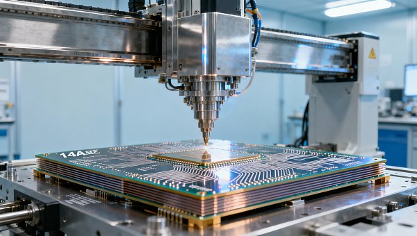
Conclusion: Intel’s 14A mass production timeline serves as a structural anchor for advanced packaging supply chain planning — not a near-term revenue driver. Its primary value is in enabling synchronized investment decisions across substrate, laminate, and assembly domains. For stakeholders, it is better understood as a synchronization point for R&D roadmaps and qualification calendars, rather than a definitive market entry indicator.
Source Attribution:
— Official statement by Intel CEO Dr. Lip-Bu Tan, May 19, 2026
— Publicly disclosed timeline: trial production in 2028, mass production in 2029
— Note: Customer names, technical specifications beyond node name, yield data, and commercial terms remain unconfirmed and require ongoing observation.
The Archive Newsletter
Critical industrial intelligence delivered every Tuesday. Peer-reviewed summaries of the week's most impactful logistics and market shifts.