Monday, May 22, 2024

How high-frequency electronics affect PCB material selection
by
Published
Views:
How High-Frequency Electronics Affect PCB Material Selection
As signal speeds rise, electronics high frequency performance becomes a decisive factor in PCB material selection. Technical evaluators must balance electrical integrity, manufacturability, thermal reliability, and sourcing risk.
The central conclusion is straightforward: standard FR-4 may remain suitable for some fast digital designs, but high-frequency applications require evidence-based laminate qualification rather than assumption.
Material selection should begin with the actual signal spectrum, interconnect length, layer construction, operating temperature, and production process, not simply a headline frequency rating.
Why High-Frequency Electronics Change the Material Decision
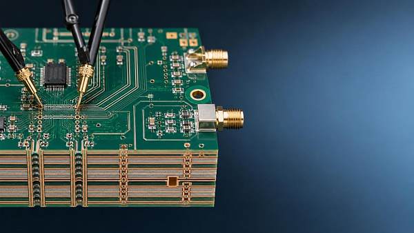
High-frequency electronics expose weaknesses that may remain invisible in lower-speed boards. Signal attenuation, impedance variation, reflections, crosstalk, and timing margin losses become more pronounced as frequency increases.
For technical evaluators, the question is not whether a material is labeled “high frequency.” The practical question is whether its measured behavior supports the complete channel budget.
A PCB is part of the electrical system, not a passive mechanical carrier. Laminate resin, glass weave, copper foil, surface finish, and stackup geometry all influence performance.
Digital systems require the same discipline as RF designs when edge rates are sufficiently fast. A clock frequency alone cannot describe the electrical stress placed on traces.
A 10 GHz signal is clearly high frequency, but a lower-frequency digital interface with sub-nanosecond transitions can also demand tightly controlled dielectric and impedance characteristics.
Evaluators should therefore define the relevant frequency range from harmonic content, protocol requirements, insertion-loss targets, and receiver margin rather than relying on nominal operating frequency.
This approach prevents over-specifying expensive materials for benign channels while avoiding false economy on links that will fail compliance, yield, or field-reliability requirements.
Start With the Electrical Requirements That Drive Risk
The first material-screening variable is dielectric constant, commonly called Dk. It determines propagation velocity and strongly affects the impedance of controlled transmission lines.
A stable Dk is often more valuable than a low published Dk. Variation across frequency, temperature, resin content, and production lot can disrupt repeatable impedance control.
Technical teams should examine the test method behind every Dk value. Results from different methods, frequencies, orientations, and cured constructions are not directly interchangeable.
Dissipation factor, or Df, indicates dielectric loss. At increasing frequencies and longer trace lengths, a higher Df contributes directly to insertion loss and reduced channel margin.
Copper loss also matters. Skin effect confines high-frequency current near the conductor surface, making copper roughness increasingly important for attenuation and phase performance.
Very rough copper can improve resin adhesion, yet its microscopic profile increases effective conductor path length. That tradeoff must be evaluated against assembly and reliability needs.
For sensitive channels, compare vendor loss data using the intended copper type and foil weight. Smooth or very-low-profile copper may materially improve performance at high frequencies.
Dielectric thickness and resin content influence impedance as strongly as basic material family. A well-designed standard laminate can outperform a poorly controlled premium stackup.
Evaluate Dk Stability, Not Just a Datasheet Number
Published Dk values are often treated as fixed constants, although real boards contain anisotropic glass reinforcement, resin-rich regions, cured resin variation, and fabrication-driven dimensional changes.
Glass weave can create local Dk variation along differential pairs. At high data rates, this effect may cause skew between conductors and reduce available timing margin.
Spread-glass constructions, pair routing angles, and appropriate layer assignments can reduce glass-weave effects. These choices must be considered jointly with laminate selection.
Dk stability over temperature deserves equal attention in automotive, industrial, outdoor, and power-electronics environments. Electrical models based only on room-temperature data can become misleading.
Moisture uptake may also alter dielectric behavior. Materials intended for humid environments should be evaluated for electrical stability after relevant conditioning, not only after dry storage.
When comparing candidate laminates, request frequency-dependent Dk data, tolerance ranges, test conditions, construction-specific information, and any available lot-to-lot process-control evidence.
For critical interfaces, use fabricator coupons and field-solver models calibrated with test data. This reduces uncertainty before committing to volume tooling or a complex qualification cycle.
Loss Budgeting Should Guide the Laminate Choice
Loss budgeting converts broad material claims into an engineering decision. It identifies whether the channel is limited primarily by dielectric loss, conductor loss, discontinuities, connectors, or package transitions.
Begin with a realistic channel model that includes trace length, via structures, reference-plane changes, connector interfaces, AC coupling components, and expected operating temperature.
Insertion-loss limits should be assessed at the frequencies that matter to the interface specification. A laminate comparison at an arbitrary low frequency can conceal real differences.
Long backplane paths, high-speed serial links, radar modules, antennas, and millimeter-wave circuits generally justify lower-loss materials earlier than short local interconnects.
Conversely, short traces on a dense processor board may not require an exotic laminate if package escape routing, vias, connectors, and layout discontinuities dominate total loss.
This distinction is commercially important. Selecting a low-loss material where it produces negligible system benefit increases cost, procurement complexity, and manufacturing qualification burden.
Material decisions should therefore identify the dominant loss contributors and quantify expected improvement. “Better electrical performance” is not enough without a link-level performance outcome.
Thermal Reliability Can Override Pure Electrical Optimization
High-frequency electronics frequently operate alongside high power density. The best low-loss dielectric is not necessarily the best production choice if it complicates thermal or mechanical reliability.
Evaluate glass transition temperature, decomposition temperature, coefficient of thermal expansion, thermal conductivity, and z-axis expansion in relation to the expected assembly and service profile.
Repeated thermal cycling stresses plated through-holes, microvias, interfaces, and copper features. Higher layer counts and HDI structures make material compatibility especially consequential.
A material with attractive Df performance may require revised lamination cycles, drilling parameters, desmear controls, or surface preparation. Those process implications belong in the qualification plan.
For power amplifiers, RF front ends, EV control electronics, and industrial drives, thermal conductivity may influence both component temperature and long-term electrical stability.
Consider the complete heat path through copper planes, dielectric layers, thermal vias, interface materials, enclosure interfaces, and airflow. Laminate conductivity alone rarely determines the outcome.
Technical evaluators should require thermal reliability evidence relevant to the intended stackup. Generic material certificates cannot replace representative coupon testing and assembly-level validation.
Stackup, Copper, and Fabrication Controls Matter as Much as Resin Chemistry
Material performance is realized through the stackup. Trace width, dielectric spacing, copper thickness, foil profile, resin flow, and pressed thickness tolerance directly affect impedance.
Controlled-impedance requirements should be communicated as a fabrication requirement with acceptable tolerance, reference structures, measurement methods, and adjustment responsibilities clearly defined.
A fabricator may alter artwork or dielectric geometry to meet impedance targets. Teams must understand whether such adjustments affect routing density, breakout feasibility, or differential-pair spacing.
Copper treatment selection requires a practical tradeoff. Lower-profile foil can reduce high-frequency loss, but adhesion, etching behavior, handling, and reliability must remain acceptable.
Surface finishes also influence RF behavior at exposed conductor regions. Their effect depends on geometry, frequency, contact needs, corrosion protection, and assembly constraints.
Via design is another frequent source of avoidable degradation. Stub length, backdrilling, antipad geometry, return-path continuity, and plating quality may outweigh small laminate differences.
For this reason, a credible electronics high frequency evaluation includes the fabricator early. Material, stackup, and process choices should be reviewed as one manufacturable system.
Build a Qualification Matrix Instead of Choosing by Brand
Brand recognition can simplify early screening, but it does not replace construction-level qualification. Comparable product families may perform differently depending on resin system, glass style, and copper options.
A qualification matrix should rank candidate materials against electrical, thermal, mechanical, processing, availability, regulatory, and lifecycle criteria using weighted requirements agreed by stakeholders.
Electrical criteria typically include Dk stability, Df, insertion-loss modeling, impedance tolerance, copper roughness compatibility, moisture behavior, and frequency-specific test evidence.
Manufacturing criteria should include minimum dielectric thickness, drillability, laser-via capability, resin flow, sequential-lamination compatibility, yield history, and available fabricator experience.
Supply-chain criteria are equally relevant for globally deployed products. Assess regional availability, approved distributor coverage, lead-time volatility, alternate constructions, and change-notification practices.
Qualification should identify acceptable substitutes before supply disruption occurs. An approved alternative may require revised impedance geometry, and that dependency must be documented in advance.
For regulated industries, include traceability, material declarations, standards alignment, and record retention. A technically capable laminate that lacks required documentation can delay product release.
Use Test Data That Matches the Actual Application
Datasheets are useful for screening, but final selection requires test evidence aligned with the intended application. Generic values may be measured under conditions unlike production use.
For RF designs, S-parameter measurements on representative transmission lines provide actionable data. They reveal insertion loss, return loss, phase response, and construction-dependent variation.
For high-speed digital channels, validate against protocol-specific masks, eye diagrams, bit-error-rate objectives, and channel operating margins. Simulated compliance alone may not be sufficient.
Test coupons should reflect actual copper type, pressed dielectric thickness, trace geometry, and fabrication process. Otherwise, measured results may falsely represent the released board.
Correlation is essential. Compare simulation models, coupon measurements, fabrication measurements, and assembled-board results to find where assumptions diverge from physical behavior.
Environmental testing should include the relevant thermal, humidity, vibration, and electrical-stress conditions. High-frequency performance must remain acceptable throughout the intended service environment.
Document lessons from each qualification. A structured evidence library shortens future sourcing decisions and helps procurement teams evaluate substitutions without repeating every engineering activity.
Common Material-Selection Errors and How to Avoid Them
A common error is selecting material solely by maximum frequency. Frequency labels do not capture trace length, rise time, loss budget, layer construction, or the dominant discontinuity.
Another error is comparing Dk and Df values without checking test methods. Inconsistent measurement conditions can make one laminate appear superior when results are not comparable.
Teams also underestimate copper roughness. A low-Df dielectric may deliver less improvement than expected when paired with a rough foil unsuitable for the operating spectrum.
Ignoring fabrication capability is equally risky. A material that performs well in laboratory samples can introduce yield loss, registration issues, drilling problems, or inconsistent press thickness.
Procurement decisions based only on unit laminate cost can create larger system costs. Redesign, compliance failure, delayed qualification, and single-source exposure usually exceed material savings.
Finally, avoid qualifying only one configuration. Multiple board thicknesses, copper weights, and resin contents can behave differently, especially when high-frequency impedance tolerances are narrow.
A Practical Decision Framework for Technical Evaluators
First, define the electrical channel requirements, including maximum relevant frequency, trace lengths, loss limits, impedance targets, timing margin, and environmental operating conditions.
Second, model the channel using realistic stackup candidates. Separate dielectric loss, conductor loss, connector loss, and discontinuity effects to identify the true design constraint.
Third, screen materials using comparable, construction-specific electrical and thermal data. Eliminate candidates that cannot meet process, availability, compliance, or lifecycle requirements.
Fourth, involve qualified fabricators to confirm stackup feasibility, impedance control capability, copper options, lamination behavior, and expected production tolerances before finalizing design rules.
Fifth, build representative coupons and validate the channel. Use measured results to refine models, confirm margin, and establish accepted fabrication controls for volume production.
Finally, establish alternate material and supplier strategies. Resilience requires technically verified options, not an informal assumption that another laminate will behave the same way.
Conclusion: Select for Verified System Performance
High-frequency electronics affect PCB material selection because electrical behavior becomes inseparable from stackup design, copper profile, fabrication control, thermal conditions, and supply-chain continuity.
Technical evaluators should resist both extremes: assuming standard FR-4 is always adequate and assuming premium low-loss materials are automatically necessary for every fast design.
The defensible choice is the material system that meets measured channel requirements with reliable manufacturing margin, verified environmental durability, practical sourcing options, and justified total cost.
By qualifying Dk stability, Df, copper roughness, thermal behavior, impedance control, and production capability together, teams can reduce redesign risk and protect long-term electronics high frequency performance.
The Archive Newsletter
Critical industrial intelligence delivered every Tuesday. Peer-reviewed summaries of the week's most impactful logistics and market shifts.